Lensless Ultra-Miniature CMOS Computational Imagers and Sensors
Abstract
We describe a new class of lensless, ultra-miniature computational imagers and image sensors employing special optical phase gratings integrated with CMOS photodetector matrices. Because such imagers have no lens, they are ultra-miniature (100 m), have large effective depth of field (1mm to infinity), and are very inexpensive (a few Euro cents). The grating acts as a two-dimensional visual “chirp” and preserves image power throughout the Fourier plane (and hence preserves image information); the final digital image is not captured as in a traditional camera but instead computed from raw photodetector signals.
The novel representation at the photodetectors demands that algorithms such as deconvolution, Bayesian estimation, or matrix inversion with Tikhonov regularization be used to compute the image, each having different bandwidth, space and computational complexities for a given image fidelity. Such imaging architectures can also be tailored to extract application-specific information or compute decisions (rather than compute an image) based on the optical signal.
In most cases, both the phase grating and the signal processing can be optimized for the information in the visual field and the task at hand. Our sensor design methodology relies on modular parallel and computationally efficient software tools for simulating optical diffraction, for CAD design and layout of gratings themselves, and for sensor signal processing.
These sensors are so small they should find use in endoscopy, medical sensing, machine inspection, surveillance and the Internet of Things, and are so inexpensive that they should find use in distributed network applications and in a number of single-use scenarios, for instance in military theaters and hazardous natural and industrial conditions.
I. INTRODUCTION
The traditional camera obscura model—in which each point in the scene is imaged onto a single point on a sensor or image plane—has dominated the science and technology of imaging systems for several millennia, at least for sources illuminated by incoherent light. The Chinese philosopher MoTi traced an inverted image produced by a pinhole camera to record an image in the fifth century B.C. [1] and Johannes Kepler traced a real image projected by a converging lens onto paper in 1603. Chemical recording of projected images, such as by mercury or silver halide, was invented in 1826 and the first true digital camera was built in 1975, [2] all these exploiting the fundamental camera obscura architecture.
The rise in digital imaging, where image processing can be incorporated into the data chain, has enabled new imaging architectures. Cathey and Dowski took an early and conceptu-ally important step away from the traditional camera obscura model by exploiting digital processing [3]. They designed a cubic-phase optical plate which, when inserted into the optical path of a traditional camera, led to an image whose (significant) blur was independent of the object depth: the image on the sensor plane did not “look good” as it would in a traditional camera obscura.
Subsequent image processing sharpened the entire blurred image, thus leading to enhanced depth of field. Since then the field of computational imaging has explored imaging architectures in which the raw signals do not superficially resemble a traditional image; instead, the final image is computed from such signals. More and more of the total imaging “burden” is borne by computation, thereby expanding the class of usable optical components. In this way, many optical aberrations can be corrected computationally rather than optically.
This imaging paradigm has led to new conceptual foundations of joint design of optics and image processing, [4] as well as a wide range of non-standard imaging architectures such as plenoptic, coded-aperture and multi-aperture systems, each with associated methods of signal processing [5]–[9].
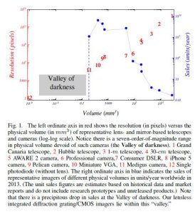
The economic pressures for miniaturization of electronic devices, including cameras, arising in the mobile computingmarket have led to smaller imager form factors [10]. Figure 1 shows the resolution, in total pixels per exposure, versus physical volume of imaging systems in the traditional camera obscura architecture (or curved mirror equivalent). While such imagers span 22 orders of magnitude in physical volume and 15 orders of magnitude in pixel resolution, the smaller the imager the greater the number sold commercially…but only down to a scale of roughly 1mm³.
There is a conspicuous gap of seven orders of magnitude in physical volume—the “Valley of darkness”—between the smallest digital camera and a single unlensed hotoreceptor. It seems that the camera obscura model has reached its physical limits and cannot be scaled much smaller. A new imaging architecture is required to span the Valley of darkness.
Recently, a new miniature imaging architecture has been explored, one based on integrating optics with CMOS photo-detectors [11]–[15]. In brief, this architecture forgoes lenses and relies instead on simple square-wave diffraction gratings created in CMOS itself. The earliest designs in this architecture relied on CMOS wires to act as amplitude optical grating patches, the gratings producing a wavelet-like representation of the scene on the sensor matrix. More recently, square-wave phase gratings have also been explored [16]. For a given image resolution, such diffractive elements enable the construction of imagers much smaller than does the basic camera obscura model. (We mention in passing that related CMOS structures have been explored for integrated spectroscopy as well [17].)
There are a number of limitations of such previous work. First, amplitude gratings based on CMOS wires have poor low-light sensitivity because most of the incident light never strikes the photodetector. Second, regular diffraction gratings are by their very nature wavelength sensitive, i.e., the pattern of light on the photodetectors depends strongly upon the wavelength of incident light. Third, such imagers are sensitive to manufacturing defects—specifically a small deviation in the thickness of the grating layer can lead to a large (and difficult to correct) alteration of the diffraction pattern on the photodetectors [13].
The method we describe here, while based on integrated silicate phase optics and CMOS image sensors, is fundamen-tally different from prior work in a number of deep ways. Our method relies on novel special phase anti-symmetric spiral phase gratings, which overcome prior limitations and afford new functionality [18]. Moreover, our new sensor architecture enables the construction of new classes of ultra-miniature sensors whose output is an estimation of some property of the scene (e.g., visual motion) or a decision (e.g., face detection or barcode reading).
We begin in Section II with a discussion of our fundamental technology and turn in Section III to a short description of our software design and analysis tools. We describe our first hardware devices in Section IV. We mention a few application areas for such sensors and imagers in Section V and conclude in Section VI with a brief summary and suggestions for future research. The results of our hardware verification of the theory and design will be presented at a later date.